3DIC Chiplet
Background

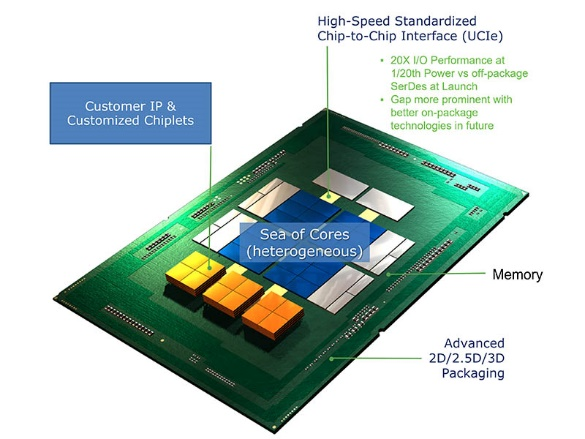
As chip manufacturing technology continues to approach physical limits, the layout design of chips - heterogeneously integrated 3DIC advanced packaging technology has become one of the best ways to continue Moore's Law. 3DIC integrates chips with different manufacturing processes and properties into a single package by a three-dimensional stacking manner and has advantages in terms of performance, power consumption, area, and cost, which provide higher levels of integration, higher performance computing, and more memory access for leading applications such as 5G mobile, HPC, AI, and automotive electronics. However, as a new field, there is no mature design and analysis solution before for 3DIC, and the use of traditional point tools and processes will bring great challenges to design convergence. The demands for signal and power integrity analysis have also exploded with the popularity of vertical stacking chip design.

Solution

Xpeedic's 3DIC Chiplet design and simulation platform consolidates multi-physics analysis capabilities within the 2.5D/3D advanced packaging, which fully supports TSMC's and Samsung's advanced packaging fabrication.
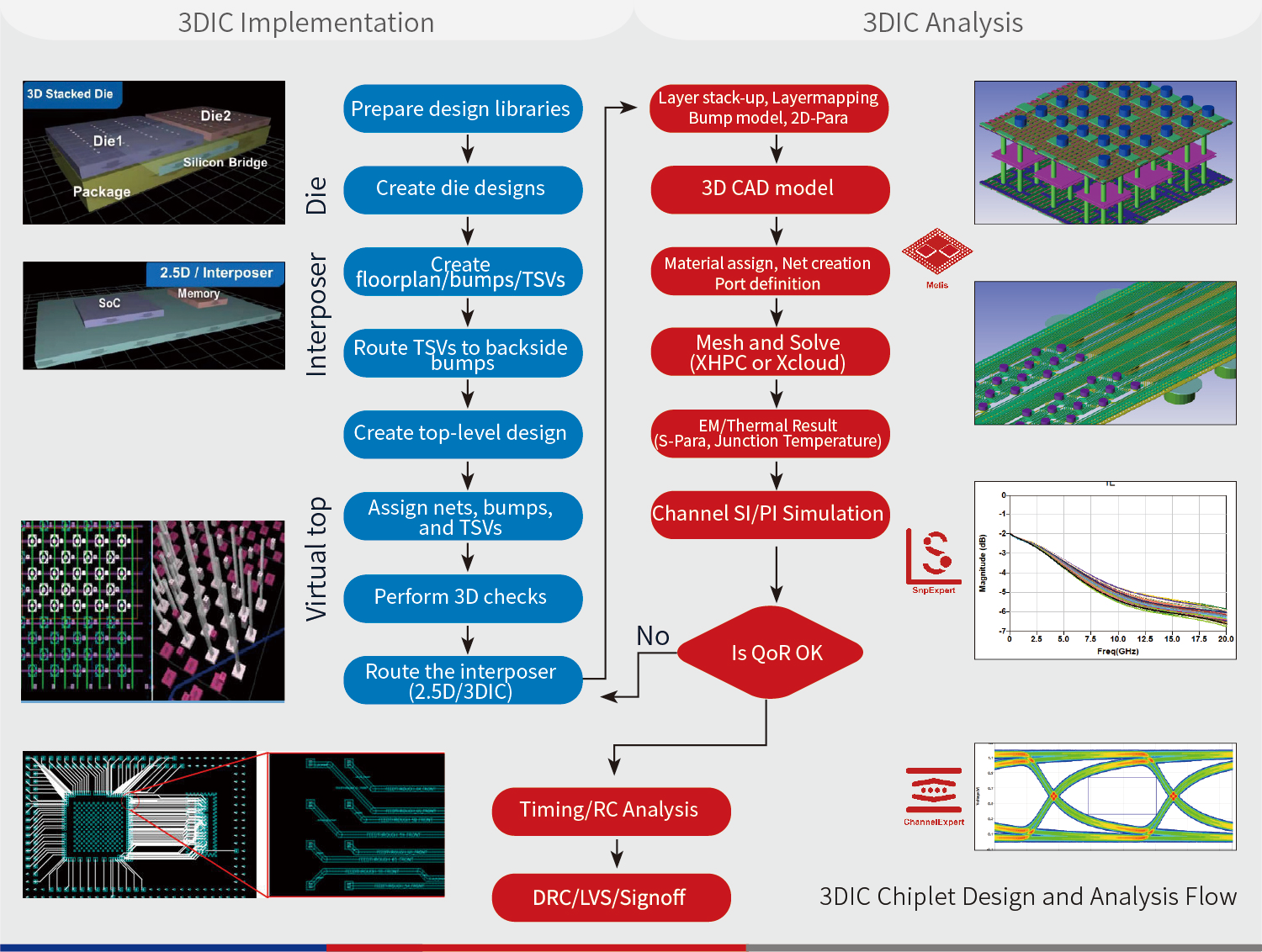
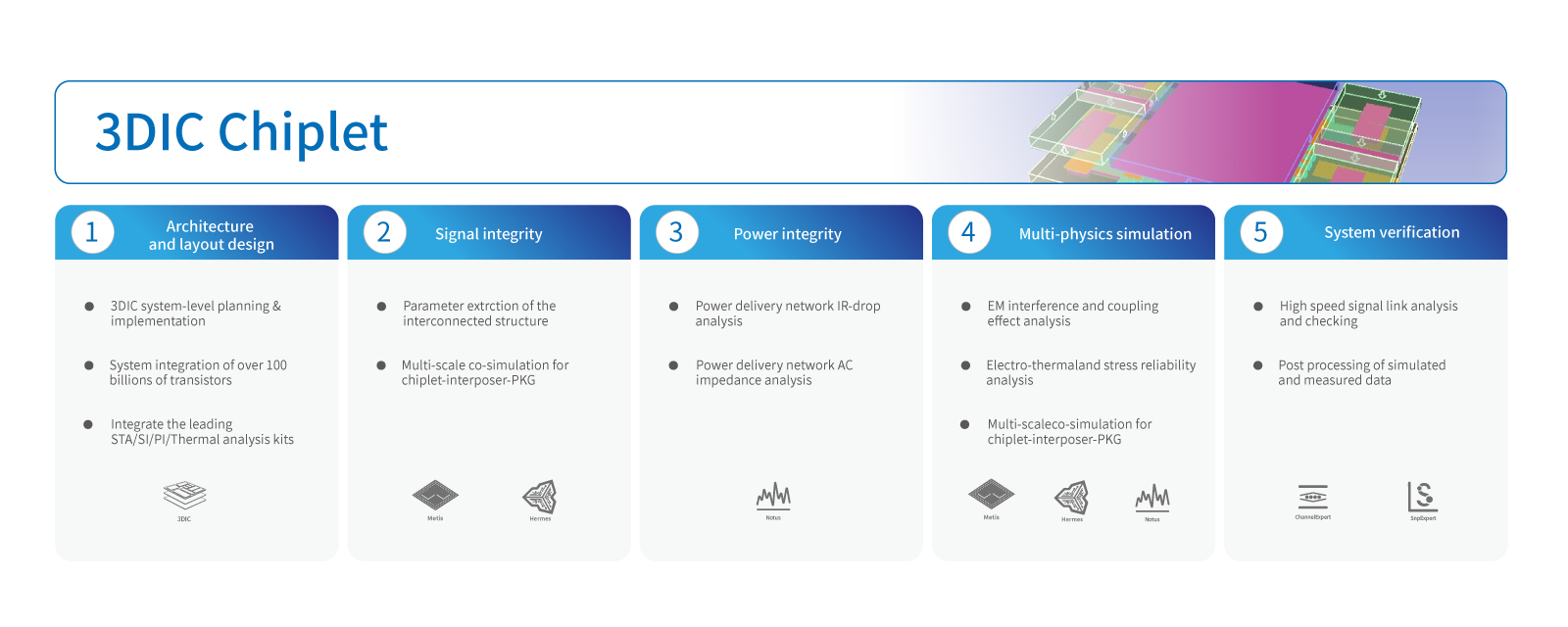
The platform provides a complete 3DIC process solution from architecture exploration, physical implementation, analysis verification, signal integrity simulation, power integrity simulation to final sign-off. It is a fully integrated and unified operation environment, which greatly improves the iteration efficiency of 3DIC design and achieves full process design & analysis automation. By pioneering the "Speed - Balance - Accuracy" three simulation modes, Metis helps engineers choose the best mode according to their application scenarios at different stages of 3DIC design so that the best solution could be quickly converged. The Xpeedic’s 3DIC Chiplet EDA Platform can support hundreds of thousands of data channels between chips simultaneously and perform collaborative simulation analysis at the chip-Interposer-packaging system level. Furthermore, the electro-thermal and stress reliability analysis is also very important and needs to be considered when high performance computing chips operate with high load. Notus multi-domain so-simulation platform includes SI/PI co-analysis, topology extraction, and thermal stress analysis for chip, packaging, and board-level designs in high-speed design. ChannelExpert, a high-speed system simulation platform, offers full-link analysis for time-domain and frequency-domain analysis in high-speed systems. It provides a fast, accurate, and simple way to evaluate, analyze, and resolve high-speed channel signal integrity issues.

Highlights

• Completely self-developed simulation engine
• Leading multi-scale simulation capabilities
• AI-driven meshing technologies
• Distributed parallel computing capabilities based on cloud computing
• Co-simulation and analysis of Chiplet-interposer-package substrate

